In SMT Process the main reason of affect the solder paste’s printing quality(Part 2)

The main functions of the stencil is printing the solder paste on the solder pad of PCB accurately . In the solder paste printing process, stencil template’s processing quality directly affect the quality of the solder paste printing, thickness of template and opening size determines the amount of solder paste printing, and stainless steel laser templates are need by outsourcing processing production. As a result, the thickness of the template and design opening parameters must be confirmed well before the outsourcing processing , to ensure that the solder paste printing quality.
Usually in a PCB there are components that lead spacing is more than 1.27 mm , also has narrow leading spacing components.
Spacing more than 1.27 mm,need 0.2 mm thickness stainless steel plate, narrow spacing components need 0.15 to 0.10 mm thickness stainless steel plate, then according to the situation of most components on PCB decided to stainless steel plate thickness, and then through the individual components welding plate to adjust the opening size of the larger or smaller leakage of solder paste printing.
If the required amount of solder paste on the same piece of PCB components disparity is bigger, the narrow spacing components of the template can be localized thinning processing, but some thinning process with higher processing cost.Therefore, can be used in a compromise, stainless steel plate thickness desirable a middle value, for example: some components on the same piece of PCB requirements 0.20 mm thick, Some other components required at 0.15- 0.12 mm thick, then the stainless steel plate can choose 0.18 mm thick. For normal components ,the opening size can be 1:1, for the large requirement of solder paste like Chip components and PLCC ,the opening area can be expanded by 10%. For the pin spacing of 0.5 mm and 0.65 mm of QFP device, the open area should be reduced 10%.
Appropriate opening shape can improve mounting effect, for example: when the Chip components size less than 1005, 0603, due to the distance between the two solder pad is very small, both ends of the solder paste easily adhesion at the bottom of the element, after reflow oven,it is easy to produce components bottom of the bridge and the weld bead. Accordingly, when processing templates, can modified a pair of rectangular pad (FIG. 1) inside opening shape into pointed horn or bow (as shown in figure 2, Chip components mouth shape), cutting down on the amount of solder paste at the bottom of the element, so that we can improve the SMT components solder paste’s bottom adhesion.


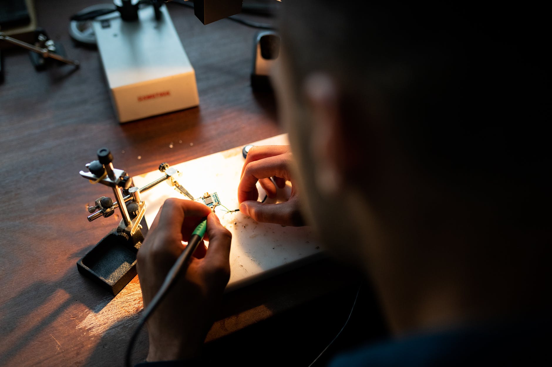
Screen Printer is equipment of printing the solder paste on the PCB , it is one of the equipments with biggest impact on the process and quality .
At present , Screen printer mainly have manual screen printer, semi-auto screen printer and full-auto screen printer.
Ø Semi-automatic printer: simple operation, fast printing speed, simple structure, the disadvantage is that: printing process parameters controlled points is less, the printing of accuracy is not high, poor solder paste release, generally applies to 0603 and above components, pin spacing bigger than 1.27 mm in PCB printing process.
Ø Fully automatic printing machine, printing with high accuracy, good effect in solder paste release, printing process is stable, is suitable for dense narrow lead spacing’s component printing;The disadvantage is that: high maintenance cost, high knowledge level requirements for operators.
–
–
–
–
Still not finish ,after will update at next post .Thanks.
–
–
–
–
–
–